Leading experts in Design Verification, FPGA Validation, RTL Design, with proven Expertise in Pre-Si and Post -Si Validation, VIP Verification, Physical Design, RF Design, and DFT.
Leading experts in Design Verification, FPGA Validation, RTL Design, with proven Expertise in Pre-Si and Post -Si Validation, VIP Verification, Physical Design, RF Design, and DFT.
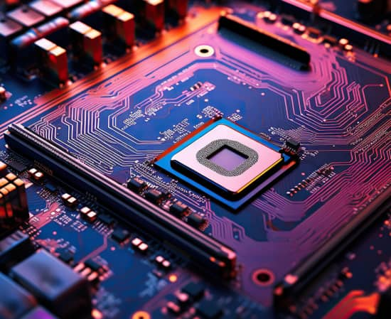
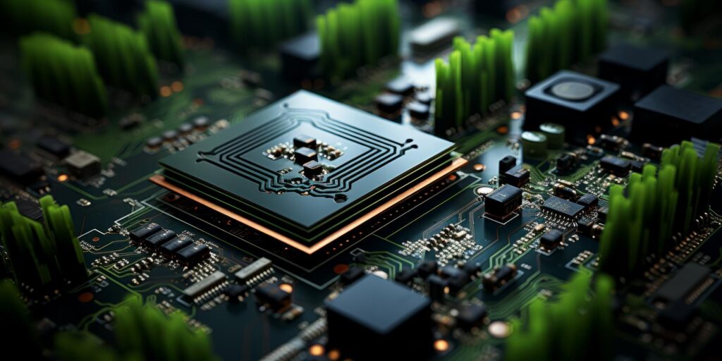
Board design, often referred to as printed circuit board (PCB) design, involves the process of designing the layout for electronic circuits on a board. This is a critical step in the development of electronic devices, ensuring that electrical components are correctly connected and that the board functions as intended. Here is a detailed look at board design, its components, and the latest trends.
Schematic Design – Represents the electrical connections between components. The tools used are CAD software like OrCAD, Altium Designer, and KiCad. Correct symbol usage, net naming, and component values are the key points to be considered.
Component Placement – The purpose is to arrange components on the board to optimize space and performance. Signal flow, thermal management, and accessibility for testing are the key points to be considers. The tools used are Layout editors in EDA software.
Routing – The purpose is to connect components with conductive traces. The different type of routing includes Manual routing and automatic routing. The points to consider are Trace width, impedance control, and avoiding crosstalk. Tools used fort this process are EDA software with advanced routing capabilities.
Layers and Stack-Up – The purpose of this key component is to Define the layers of the PCB, including signal, power, and ground layers. The different types of Single-layer, double-layer, and multi-layer boards. Layer count, material selection, and via usage are the key points to consider.
Power and Ground Planes – The purpose is to provide stable power distribution and minimize noise. The key areas to focus during this phase are Plane segmentation, decoupling capacitors, and grounding strategy.
Signal Integrity – The purpose is to ensure signal quality throughout the PCB. Focus areas to consider in this area are Trace impedance, differential pairs, and termination. There are tools available for use such as Signal integrity analysis software.
Thermal Management: The purpose of this is to dissipate heat generated by components. The various techniques available and in use are Heat sinks, thermal vias, and copper pours. The key things to consider are component placement and airflow.
Manufacturability – design for ease of manufacturing and assembly. Key considerations in this component are design for manufacturing (DFM), design for assembly (DFA), and panelization. DFM analysis software are the tools used.
High-Density Interconnect (HDI) – PCBs with a higher density of interconnections. The associated benefits are Reduced size, increased performance, and support for advanced features. The various techniques are Microvias, blind and buried vias, and finer trace/space dimensions.
Flexible and Rigid-Flex PCBs – Boards that can bend and twist, combining rigid and flexible substrates. Wearables, medical devices, and compact electronics are some of the application areas. The benefits associated are Space-saving, weight reduction, and enhanced durability.
Embedded Components – Integrating passive and active components within the PCB layers. The benefits involved are Reduced size, improved electrical performance, and better thermal management. Some of the challenges involved with this are manufacturing complexity and cost.
High-Frequency and High-Speed Design – The importance is it supports applications like 5G, high-speed data transfer, and RF communication. However, the important key points to consider in this method are controlled impedance, low-loss materials, and careful routing.
The tool available is high-frequency simulation and modelling software.
Advanced Materials – The latest trends use materials like Rogers, PTFE, and ceramic substrates. The associated benefits include lower dielectric loss, better thermal performance, and high-frequency stability. The various applications are RF and microwave circuits, high-speed digital circuits.
3D Printing and Additive Manufacturing – The trend is to use 3D printing technology to create PCBs. The benefits associated are rapid prototyping, complex geometries, and reduced waste. The various applications can be found are custom and low-volume production, innovative form factors.
Internet of Things (IoT) Integration – The requirements are in the areas such as Low power consumption, wireless connectivity, and compact design. The Technologies used are Embedded antennas, energy harvesting, and miniaturized components.
Environmental and Sustainability Considerations – The latest trends are to use Eco-friendly materials, lead-free soldering, and energy-efficient designs. The standards to follow are RoHS (Restriction of Hazardous Substances) and WEEE (Waste Electrical and Electronic Equipment).
AI and Machine Learning in PCB Design – The application areas are automated layout optimization, predictive maintenance, and design rule checking. The benefits associate are improved design accuracy, reduced time-to-market, and enhanced performance.
The challenges involved in Board Design are
Complexity Management – Handling the increased complexity of modern electronic systems and using hierarchical design and modularization to simplify the process.
Signal and Power Integrity – Ensuring high-speed signals maintain integrity across the PCB and managing power distribution networks to minimize noise and voltage drops.
Thermal Issues – Addressing heat dissipation in densely packed boards and using thermal simulations to predict and mitigate hot spots.
Manufacturing Constraints – Designing within the capabilities of PCB manufacturers and Ensuring design files are ready for production with minimal adjustments.
Cost Management – Balancing performance requirements with budget constraints and optimizing material choices and manufacturing processes to reduce costs.
Board design is a rapidly evolving field driven by advancements in technology and increasing demands for more complex and efficient electronic devices. Staying updated with the latest trends and integrating advanced tools and techniques is crucial for developing high-performance, reliable, and cost-effective PCBs. As technology continues to advance, board design will remain a fundamental aspect of innovation in the electronics industry.