Leading experts in Design Verification, FPGA Validation, RTL Design, with proven Expertise in Pre-Si and Post -Si Validation, VIP Verification, Physical Design, RF Design, and DFT.
Leading experts in Design Verification, FPGA Validation, RTL Design, with proven Expertise in Pre-Si and Post -Si Validation, VIP Verification, Physical Design, RF Design, and DFT.
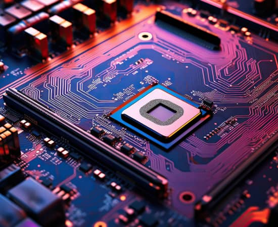
Design for Testing (DFT) in VLSI refers to the process of designing semiconductor chips in a way that facilitates efficient testing of the manufactured devices. The primary goal of DFT is to ensure that all potential faults within the design can be detected and diagnosed during the manufacturing test process

Scan Design – Involves inserting scan chains into the design, which allows for serial access to internal flip-flops during testing. This process facilitates the application of test patterns and the capture of test responses for comprehensive fault detection. The different techniques used are Scan chain insertion, scan compression techniques (like Test Compression Logic), and ATPG (Automatic Test Pattern Generation) tools to generate efficient test patterns.
Built-In Self-Test (BIST) – Integrates test pattern generation and response collection circuitry within the design itself. It reduces external test equipment requirements and enables on-chip testing without relying heavily on ATE resources. Implementations include BIST controllers, test pattern generators (TPG), and response analyzers (TAR) designed to handle specific test algorithms.
Boundary Scan (JTAG) – Standardized interface (IEEE 1149.1) for testing interconnects and verifying external connections of ICs. This enables testing of PCB-level interconnects, verifying the integrity of pins, and facilitating board-level debugging. This is useful for testing devices with complex I/O configurations and for in-system programming and debugging.
Design Structure Modifications – Includes adding test points, observability points, and design re-structuring to enhance testability. It improves fault coverage and reduces the complexity of test pattern generation.

Scan-Based Testing – It involves shifting test patterns through scan chains to observe responses and detect faults. The advantages are High fault coverage, suitable for detecting stuck-at faults and other static faults. The challenges involved are, it increases test data volume and test application time, necessitating efficient compression techniques.
BIST Techniques – Different types are Memory BIST (MBIST) for testing embedded memories, Logic BIST for testing combinational logic, and hybrid BIST combining both. The advantage is, it reduces reliance on external test equipment, improves fault coverage, and enables testing of inaccessible parts of the design.
Advanced ATPG and Test Compression – This utilizes sophisticated ATPG algorithms to generate efficient test patterns that cover a wide range of faults. This method reduces the size of test patterns to minimize test time and data volume while maintaining high fault coverage.
Hierarchical DFT – Applies DFT techniques at different hierarchical levels of the design to manage complexity and optimize testability. This process enhances scalability, facilitates reuse of test structures, and improves overall test efficiency.
AI/ML in DFT – Utilizes machine learning algorithms for test pattern generation, fault diagnosis, and test coverage optimization. The advantage is, it improves efficiency by automating complex tasks and enhancing fault detection capabilities.
Security-Focused DFT – Integrates DFT techniques for testing security features and detecting vulnerabilities (e.g., side-channel attacks, hardware Trojans). It incorporates security-aware testing and compliance with security standards (e.g., ISO/IEC 15408 Common Criteria).
High-Level Synthesis (HLS) for DFT – It applies HLS techniques to generate DFT structures directly from high-level behavioral descriptions (C/C++/SystemC). The benefit of this is it accelerates DFT implementation, improves design productivity, and facilitates early validation of test structures.
DFT for AI/ML Accelerators – Develops tailored DFT strategies for AI/ML accelerators, addressing unique testing challenges such as deep neural network (DNN) inference engines.
Cloud-Based DFT Solutions – Utilization of cloud-based platforms for scalable ATPG, test pattern simulation, and validation, enabling faster turnaround times and resource optimization.
Post-Silicon DFT – Enhances DFT techniques for post-silicon debug and diagnosis, leveraging built-in capabilities for on-chip monitoring and error reporting. DFT plays a crucial role in ensuring the quality and reliability of VLSI designs by enabling comprehensive testing and fault detection during manufacturing. The latest trends in DFT focus on integrating advanced technologies such as AI/ML, HLS, security-focused testing, and cloud-based solutions to enhance test efficiency, reduce time-to-market, and address the growing complexity of semiconductor designs. Keeping abreast of these trends allows semiconductor companies to adopt cutting-edge DFT methodologies and tools, thereby improving overall product quality and reliability while optimizing test costs and time.