

In the fast-paced world of semiconductor innovation, the success of any chip design hinges not just on its creativity but on its accuracy and reliability. With billions of transistors integrated on a single chip, VLSI (Very Large Scale Integration) Design Verification becomes a mission-critical step in ensuring that the intended functionality is delivered before fabrication. Missing a fault at this stage can cost millions of dollars and result in months of redesign. This is why leading-edge companies invest heavily in robust verification strategies.
At Vaaluka Solutions, our mission is to empower semiconductor innovators with high-quality verification services that prevent costly errors and accelerate time-to-market.
How VLSI Design Flow Works?
To understand where design verification fits in, it’s helpful to take a quick look at the VLSI design flow.
A typical flow includes:
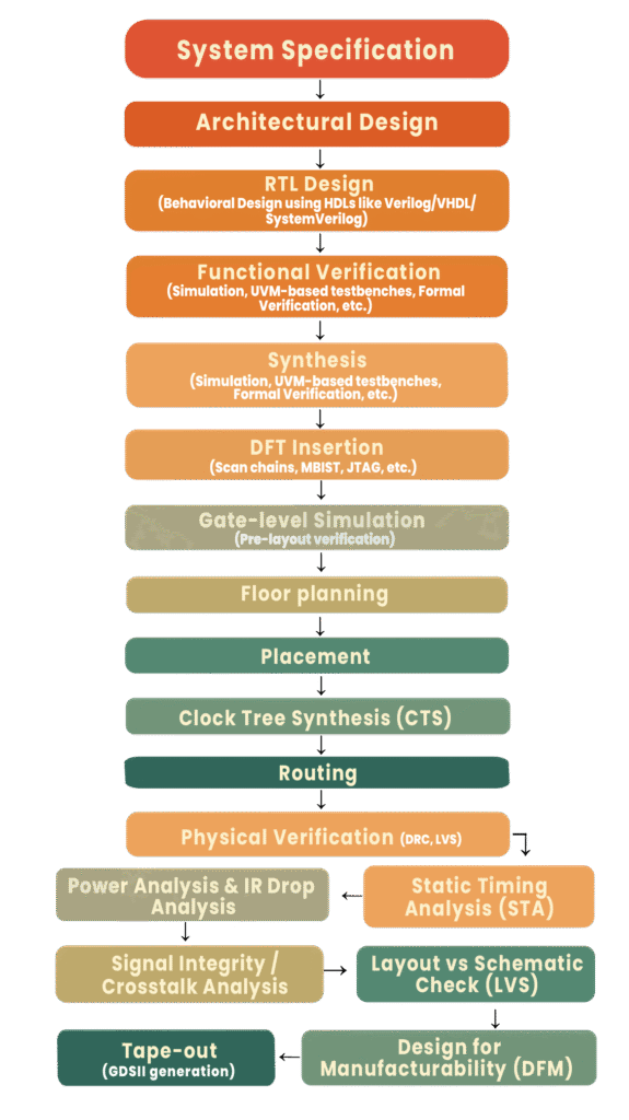
Stage | Description |
System Specification | Define system-level requirements like functionality, performance, area, power, and I/O standards. |
Architectural Design | Choose microarchitecture, partition blocks, define pipelines, memory hierarchy, etc. |
RTL Design | Describe functionality using HDLs like Verilog/VHDL. |
Functional Verification | Simulate RTL using UVM/Testbenches, assertions, or formal methods. |
Synthesis | Convert RTL to gate-level netlist using synthesis tools. |
DFT Insertion | Insert scan chains, BIST, boundary scan (JTAG). |
Gate-Level Simulation (GLS) | Verify synthesized netlist for timing and logic correctness. |
Floor-planning | Define block placement areas, I/O locations, and power grids. |
Placement | Place standard cells and macros. |
Clock Tree Synthesis (CTS) | Balance clock distribution and minimize skew. |
Routing | Connect all signals using metal layers. |
Physical Verification | Ensure design adheres to DRC and LVS rules. |
Static Timing Analysis (STA) | Validate timing across PVT corners. |
Power & IR Drop Analysis | Check power integrity and voltage drops. |
Signal Integrity / Crosstalk Analysis | Identify and mitigate noise and interference. |
LVS (Layout vs Schematic) | Match layout with logical netlist. |
Design for Manufacturability (DFM) | Ensure layout can be reliably fabricated. |
Tape-out | Generate final GDSII file for fabrication. |
Verification begins early in the RTL phase and continues across multiple stages to ensure design correctness before it’s handed off for physical implementation.
What is VLSI Design Verification?
VLSI Design Verification is the process of ensuring that the design behaves as expected and meets all functional requirements before fabrication. It’s not just about finding bugs—it’s about building confidence in the design.
Verification encompasses several types:
- Functional Verification – testing the logic against the functional spec
- Formal Verification – mathematically proving the correctness of design properties
- Emulation & FPGA Prototyping – simulating large designs at near-real speeds
- Static Checks – identifying issues like uninitialized variables, clock domain crossing errors, and more
- Gate-Level Netlist Simulations – These simulations are performed after synthesis, using the gate-level representation of the design. They help verify that the synthesized netlist still meets functional and timing expectations, particularly under real timing delays and constraints. This step is essential to detect issues like race conditions and glitches that are not visible at the RTL level.
Without thorough verification, a design might work in simulation but fail in real-world conditions, something no product team can afford.
Key Verification Methodologies & Tools
As chips become increasingly complex, structured methodologies and advanced tools become indispensable.
Key Methodologies:
- UVM (Universal Verification Methodology): The industry-standard approach that enables modular, reusable, and scalable testbenches.
- Constraint Random Verification: A methodology that uses randomized input generation within defined constraints to uncover unexpected design behaviors.
- Functional Coverage: A technique to measure which parts of the design and test scenarios have been exercised to ensure thorough verification.
- Code Coverage Analysis: Used to determine how much of the verification code and design logic has been exercised by the test suite, helping identify untested areas.
- Design for Verification (DfV): A design approach focused on making designs easier to verify, improving testability and reducing verification time.
- Coverage-Driven Verification (CDV): Ensures that every possible corner case is exercised.
Commonly Used Tools:
- Synopsys VCS
- Cadence Xcelium/Incisive
- Mentor Graphics Questa
- JasperGold (for formal verification)
At Vaaluka Solutions, our verification engineers are proficient in these tools and tailor the methodology to suit the design’s scale and complexity.
Challenges in VLSI Verification
Verification often consumes up to 70% of the total design effort, and for good reason. Key challenges include:
- Time-to-Market Pressure: As product cycles become shorter, verification must be both comprehensive and efficient.
- Scalability: Modern SoCs with multiple IPs require reusable and scalable test environments.
- Debug Complexity: Identifying root causes of failures in large simulation datasets can be daunting.
- Coverage Closure: Achieving complete functional coverage while avoiding redundancy requires expertise and planning.
Vaaluka Solutions addresses these challenges by adopting automation, coverage planning, and modular verification architectures that streamline debugging and accelerate coverage closure.
What are the Trends Shaping the Future of Design Verification?
The VLSI industry is constantly evolving, and so are verification practices. Some trends shaping the future include:
- AI/ML in Verification: From automatic test generation to intelligent debugging, AI is beginning to optimize various parts of the verification cycle.
- Shift-left Verification: Integrating verification earlier in the design cycle using continuous integration practices.
- Cloud-based Verification: Harnessing scalable cloud infrastructure to reduce simulation turnaround time.
- Portable Stimulus Standard (PSS): Enabling stimulus reuse across block-level and system-level verification.
Staying ahead of these trends enables companies to deliver first-time-right silicon, the ultimate goal of any semiconductor design team.
How Vaaluka Solutions Leads in VLSI Design Verification
At Vaaluka Solutions, we don’t just execute testbenches, we engineer confidence. Our team brings deep domain expertise, covering block-level, system-level, and SoC-level verification for various application domains, including IoT, automotive, and consumer electronics.
What sets us apart:
- Expertise in UVM-based verification frameworks
- Customizable testbench architectures for rapid onboarding of IPs
- Integrated coverage analysis and debugging workflows
- Seamless collaboration with clients for agile delivery
We partner with design teams to seamlessly integrate into their workflows and accelerate tape-out timelines without compromising quality.
Conclusion
VLSI Design Verification is more than just a step in the design flow; it’s the backbone of reliable, high-performance chip development. As designs become more complex, the verification effort must also evolve in sophistication.
Whether you’re a startup building your first chip or an established player scaling your SoC portfolio, partnering with experts like Vaaluka Solutions can ensure your silicon success. Our tailored verification strategies, skilled engineers, and domain-centric approach make us a trusted ally in your semiconductor journey.