

We’ve all been there, your device is running out of battery faster than you can say, “low power mode.” But for a hardware engineer, the real challenge isn’t just making things work. It’s making things work efficiently, using as little energy as possible.
This is where Low Power design comes in. It’s crucial practice in modern chip design that ensures your device doesn’t just perform well, it performs well without draining unnecessary power.
Types of Power Consumption in Digital Chips
- Dynamic Power (Switching Power): Dynamic power is consumed when signals toggle from 0 → 1 or 1 → 0. It increases with the switching activity, higher voltages, and higher frequencies. P_dynamic = α · C · V² · f
- Static Power (Leakage Power): Static power is consumed even when the chip isn’t switching. It arises due to leakage currents through transistors.
In this blog, we’ll explore the fundamental concepts of low-power design and dive into concepts like Clock Gating, Power Gating (PG), DVFS and how these concepts are the unsung heroes in the world of low-power design.
Key Terms You Must Know
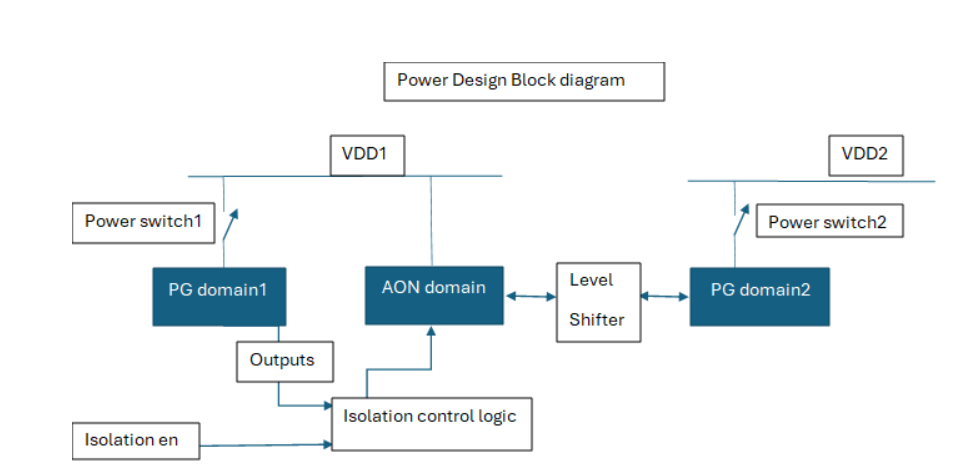
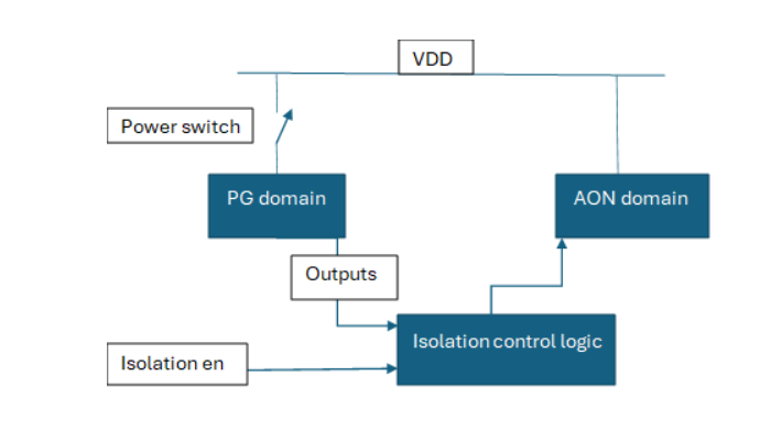
- Power Domain / Power Island: A power domain (or power island) is a section of the chip that can have its own power control. It can be turned ON/OFF independently. It may run at a different voltage.
- Always-On Domain (AON): A domain that never powers off. It contains: Power controller (PMU), Wake-up logic, Reset controllers, etc.
- Power Gating: Turning OFF a power domain to save power using a power switch.
- Power Switch: A hardware switch that disconnects VDD from a domain. Controlled by a power gate enable signal.
- Isolation Cells: Special logic inserted on signals that go from a power-off domain → to an active domain. They prevent X (unknown) values from leaking out.
When domain is OFF → outputs are clamped to 0 or 1.
When domain is ON → signals pass normally.
- Retention Cells (Retention Registers): Registers that keep their value even when the domain is powered OFF, using a small always-on backup supply.
- Retention Save/Restore
Save: Before powering down, the register saves its data into the retention latch.
Restore: After power-up, data is copied back to the main register.
- Level Shifters : Cells used when signals cross between different voltage domains.
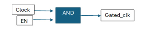
Clock Gating
Clock Gating is like having an on/off switch for your clock signals. In digital circuits, the clock is what drives the data. But sometimes, not all parts of your chip need to be “ticking” all the time.
How does it work?
Clock Gating works by disabling the clock signal to parts of the circuit that aren’t doing anything at a given moment. If a block of your chip doesn’t need to perform any operation, there’s no need to keep the clock signal running for it. This essentially freezes that block, saving power. Let’s say you’re working on a design with multiple functional blocks. By turning off the clock signal to blocks that aren’t performing operations, you avoid wasting power, and your chip stays cooler and more efficient. Reduces Dynamic power consumption.
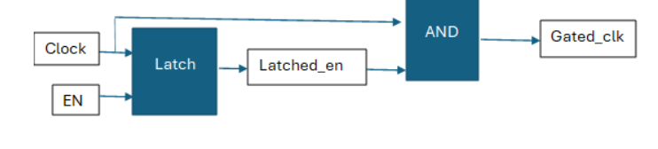
Below is a sample AND based Clock gating, but If EN changes near a clock edge, the AND gate may produce glitches.
Adding a latch ensures that the enable is stable around the clock edge, preventing glitches.
Power Gating: The Sleep Mode for Circuits
Next on the list is Power Gating, which is kind of like taking a nap for parts of your circuit. While clock gating turns off the clock to save power, power gating goes a step further: it completely disconnects the power supply to certain areas of the chip.
How does it work?
Power gating uses sleep transistors to cut off power to unused blocks. This significantly reduces the dynamic power consumption when certain parts of the chip are idle or inactive. In a smartphone, when you’re not using the camera, the power to the camera block gets shut off. Not just the clock, everything! When you open the camera app again, the power is reconnected.
It helps reduce Static power consumption. It Turns OFF power to transistors → leakage ~0
Power Down/Up Sequences: Timing is Everything
Now that we’ve talked about shutting things down, let’s focus on the Power Down and Power Up sequences. These are the delicate moves that determine how your chip gracefully enters and exits low power states.
How does it work?
When you put a chip in a low-power state, you need to shut it down in an orderly way, making sure everything is properly powered off without causing damage. Likewise, when you bring it back up, you don’t just slam everything on at once. There’s a sequence to follow to make sure everything powers back up safely and efficiently.
Power-Down Sequence (Turning OFF a Power Domain)
The order is extremely important. If you turn OFF the domain too early, you get X-propagation, data loss, or corruption.
- Initiate power-down request : PMU commands domain to shut down.
- Gating the clock : Stop the clock to reduce dynamic activity.
- Assert Save (Retention Save) : Copy register values into retention cells (if needed).
- Assert Isolation: Isolation cells clamp outputs to avoid X-prop leakage.
- Turn OFF Power Switch : Power domain becomes OFF, Signals from this domain now become X (isolated).
- Acknowledge Power-Down Complete : PMU knows the domain is fully shut down.
Power-Up Sequence (Turning ON a Power Domain)
- Turn ON Power Switch: Domain receives VDD.
- Wait for Power-Good: Ensure voltage is stable.
- Release Reset : Let logic initialize.
- Restore Retention Registers: Restore state from retention if applicable.
- Enable Clock: Clock starts running again.
- Deassert Isolation: Allow domain outputs to drive downstream logic.
- Acknowledge Power-Up Complete: PMU confirms that the domain is operational.
DVFS (Dynamic Voltage and Frequency Scaling): The Smart Power Manager
DVFS, the Dynamic Voltage and Frequency Scaling, is the master of power optimization.
What is DVFS?
DVFS is like having a super smart energy manager that adjusts your chip’s voltage and clock frequency depending on its workload. If your chip is performing a heavy task (like playing a high-definition video or running a game), it’ll need more power, so the voltage and frequency go up. When it’s idle or doing light work, the power consumption drops because the voltage and frequency decrease.
Why does it matter?
This dynamic adjustment helps you maintain optimal performance while ensuring minimum power consumption. It’s like giving your chip the flexibility to decide when it needs to speed up or slow down, and adjust its power accordingly.
In practical terms, DVFS can be used to fine-tune the performance-to-power ratio, meaning you’re not running your chip at full power all the time. This is super useful in mobile devices, where battery life is precious.
Conclusion
Low-power design techniques in VLSI have become indispensable in modern electronics. From clock gating and power gating to DVFS. These strategies provide a robust framework for optimizing power consumption. By adopting a comprehensive methodology and performing rigorous verification, designers can create VLSI circuits that are both energy-efficient and high-performing, meeting the demands of today’s mobile, IoT, and high-performance applications.